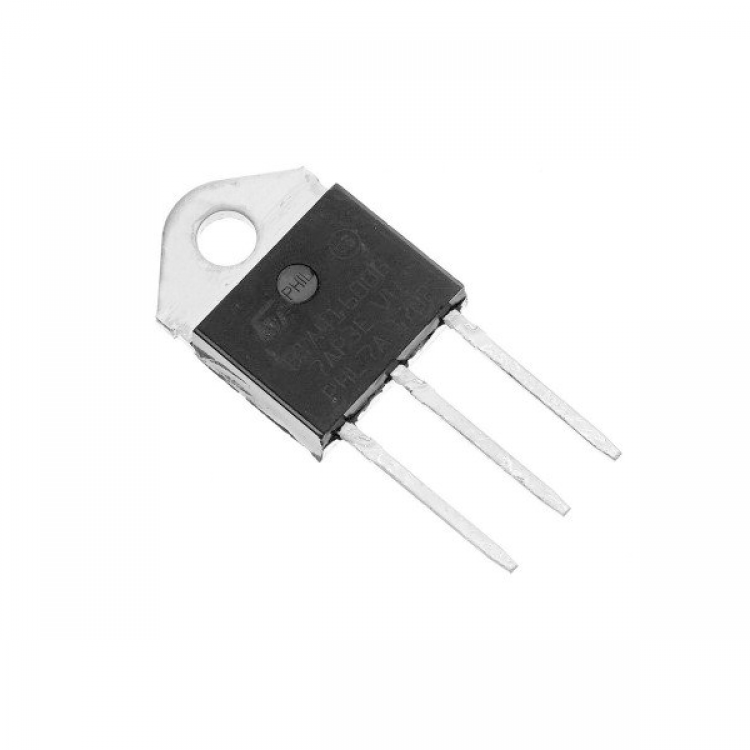


IGBT 30N60
The YR30N60P the silicon N-channel Enhanced VDMOSFETs, is obtained by the self-aligned planar Technology which reduce the conduction loss, improve switchingperformance and enhance the avalanche energy. The transistor can be used in various power switching circuit for system miniaturiz
ation and higher efficiency. which accords with the RoHS.
Features
VDS=600V;ID=30A@ VGS=10V;Typ RDS(ON) = 0.19Ω
RDS(ON)<0.22Ω @ VGS=10V
Fast Switching
ESD Improved Capability
Low Reverse transfer capacitances(Typical:44pF)
100% Single Pulse avalanche energy Test
Application
Power switch circuit of adaptor and charger.
Package Marking and Ordering Information
| Device Marking | Device | Device Package | Reel Size | Tape width | Quantity |
| YR30N60P | YR30N60P | T0-247 | - | - | - |
Absolute Maximum Ratings (TA=25℃unless otherwise noted)
| Symbol | Parameter | Value | Unit |
| VDS | Drain-Source Voltage (VGS=0V) | 600 | V |
| VGS | Gate-Source Voltage (VDS=0V) | ±30 | V |
| ID(DC) | Drain Current (DC) at Tc=25℃ | 30 | A |
| ID(DC) | Drain Current (DC) at Tc=100℃ | 20 | A |
| IDM(a1) | Drain Current-Continuous@ Current-Pulsed | 120 | A |
| dv/dt(a3) | Peak Diode Recovery Voltage | 5 | V/ns |
| PD | Maximum Power Dissipation(Tc=25℃) | 230 | W |
| Derating Factor | 1.84 | W/℃ | |
| EAS(a2) | Single Pulse Avalanche Energy | 2500 | Mj |
| TL | MaximumTemperature for Soldering | 300 | ℃ |
| TJ,TSTG | Operating Junction and Storage Temperature Range | -55 To 150 | ℃ |
General Description
package type: To-220
The TO-220 package outline is an in-line package that is commonly used in high-power transistors, small and medium-sized integrated circuits, and the like.
Among them, TO is an abbreviation of Transistor Outline. Usually, the TO-220 is a single-row in-line, which can usually lead to 3, 5 or 7 feet.
Watch this video it will give you a clear idea about this product.
Related Product